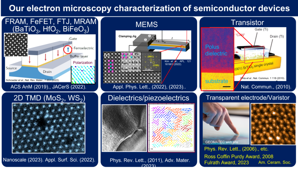
研究内容
Precise atomic position measurement
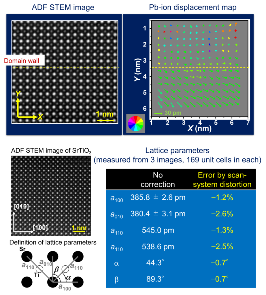
We are able to measure atomic position precisely in an atomic-scale STEM (scanning transmission electron microscopy) image. This technique is, for example, useful to map out electrical polarization in ferroelectrics (ACS Appl. Nano Mater., 2, 5761 (2019)., J. Mater. Sci., 56, 1621 (2021).). Further, lattice parameter can be measured accurately by properly correcting image distortions, by doing so, a few percent errors, which are usually expected from atomic-scale STEM measurement (J. Mater. Sci., 55, 8123 (2020).) can be considerably reduced (Phys. Status Solidi RRL, 14, 1900488 (2020).).
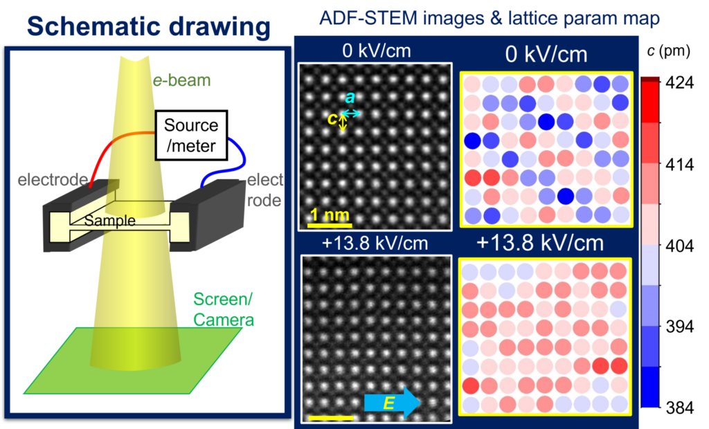
In-situ electrical biasing electron microscopy
We are able to observe electron microscopy image under an electrical stimulus to a sample (Appl. Phys. Lett. 100, 172902 (2012).). Nanoscale dynamics can be observed in real time as can seen in a movie below (Phys. Rev. Lett. 107, 187601 (2011).). Atomic-resolution observations are also possible (Appl. Phys. Lett., 111, 082905 (2017).), and atomic-scale electrostrain measurement was reported. (Phys. Status Solidi RRL, 14, 1900488 (2020).)
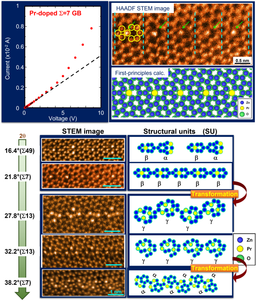
Atomic structure and electrical properties of zinc oxide grain boundaries
In this study, we aim to clarify the relationship among atomic arrangement, dopant position, electronic structure, and electrical transport across grain boundaries in zinc oxide. Structure formation mechanisms, role of dopant on nonlinear current-voltage properties have been clarified. (Phys. Rev. Lett., 97 106802 (2006)., J. Am. Ceram. Soc. 90 337 (2007)., Phys. Rev. B 87 140101 (2013). J. Am. Ceram. Soc. 98 1932 (2015).)